CHAPTER: 1
INTRODUCTION
As the sources of conventional energy deplete day by day, resorting to alternative sources of energy like solar and wind energy has become need of the hour.
Solar-powered lighting systems are already available in rural as well as urban areas. These include solar lanterns, solar home lighting systems, solar streetlights, solar garden lights and solar power packs. All of them consist of four components: solar photovoltaic module, rechargeable battery, solar charge controller and load.
In the solar-powered lighting system, the solar charge controller plays an important role as the system’s overall success depends mainly on it. It is considered as an indispensable link between the solar panel, battery and load.
The microcontroller-based solar charge controller described here has the following features:
1. Built-in digital voltmeter (0V-20V range)
2. Overcharge protection
3. System status display on LCD
4. Low current consumption
5. Highly efficient design based on microcontroller
LCD module: The system status and battery voltage are displayed on an LCD based on HD44780 controller. The backlight feature of the LCD makes it readable even in low light conditions. The LCD is used here in 4-bit mode to save the microcontroller’s port pins. Usually the 8-bitmode of interfacing with a microcontroller requires eleven pins, but in 4-bit mode the LCD can be interfaced to the microcontroller using only seven pins.
Solar panel: The solar panel used here is meant to charge a 12V battery and the wattage can range from 3 to 40 watts. The peak unloaded voltage output of the solar panel will be around 19 volts. Higher-wattage panels can be used with some modifications to the controller unit.
Rechargeable battery: The solar energy is converted into electrical energy and stored in a 12V lead-acid battery. The ampere-hour capacity ranges from 5 Ah to 100 Ah.
Rechargeable battery: The solar energy is converted into electrical energy and stored in a 12V lead-acid battery. The ampere-hour capacity ranges from 5 Ah to 100 Ah.
Charge control: Relay RL1 connects the solar panel to the battery through diode D1. Under normal conditions, it allows the charging current from the panel to flow into the battery. When the battery is at full charge (12.0V), the charging current becomes ‘pulsed.’ To keep the overall current consumption of the solar controller low, normally-closed (N/C) contacts of the relay are used and the relay is normally in de-energised state.
Load control: One terminal of the load is connected to the battery through a relay. This relay will control the load providing. That is if the resistance of load is below 3ohms(high current) then the relay get energised and cut off the load.
Load control: One terminal of the load is connected to the battery through a relay. This relay will control the load providing. That is if the resistance of load is below 3ohms(high current) then the relay get energised and cut off the load.
CHAPTER : 2
BLOCK DIAGRAM
Figure1:block diagram.
2.1) BLOCK DIAGRAM EXPLANATION
Here we are using PIC16F877A as the major component. Which will control all actions and provide basic protection based on the program.
We have a 12V rechargeable battery and a 12V solar panel ,on day time the solar panel will provide 12V ,which will charge the battery and provide 12V constant load.The charging is controlled by the Relay 1.If the battery is full then the relay get energized. So Relay 1 will provide over charge protection.
The relay switch RL2 is used to protect the battery from over load. When an overload is occurred, the relay switch RL2 is energised and it disconnects load from battery. The relay will be de-energised when the overload reset switch is pressed.
The voltage at the battery is continuously displayed on the LCD using the built-in ADC module in the PIC 16F877A. The voltage is divided by 3 by using 3 equal value resistors and 1/3 voltage is send to ADC input.
CHAPTER : 3
MICRO CONTROLLER
A microcontroller is a computer-on-a-chip, or, preferably, a single-chip computer. Micro suggests that the device is small, and controller tells you that the device might be used to control objects, processes, or events. Another term to describe a microcontroller is embedded controller, because the microcontroller and its support circuits are often built into, or embedded in, the devices they control.
Microcontrollers are found in all kinds of things these days. Any device that measures, stores, controls, calculates, or displays information is a candidate for putting a microcontroller inside. The largest single use for microcontrollers is in automobiles—just about every car manufactured today includes at least one microcontroller for engine control, and often more to control additional systems in the car. In desktop computers, you can find microcontrollers inside keyboards, modems, printers, and other peripherals. In test equipment, microcontrollers make it easy to add features such as the ability to store measurements, to create and store user routines, and to display messages and waveforms. Consumer products that use microcontrollers include cameras, video recorders, compact-disk players, and ovens. And these are just a few examples.
A micro controller is similar to the microprocessor inside a personal computer. Examples of microprocessors include Intel’s 8086, Motorola’s 68000, and Zilog’s Z80, ATMEL 89c51. These microprocessors and microcontrollers contain a central processing unit, or CPU. The CPU executes instructions that perform the basic logic, math, and data-moving functions of a computer. To make a complete computer, a microprocessor requires memory for storing data and programs, and input/output (I/O) interfaces for connecting external devices like keyboards and displays.
In contrast, a micro controller is a single-chip computer because it contains memory and I/O interfaces in addition to the CPU. Because the amount of memory and interfaces that can fit on a single chip is limited, microcontrollers tend to be used in smaller systems that require little more than the microcontroller and a few support components.
PIC micro controllers are low-cost computers-in-a-chip; they allow electronics designers and hobbyists add intelligence and functions that mimic big computers for almost any electronic product or project.
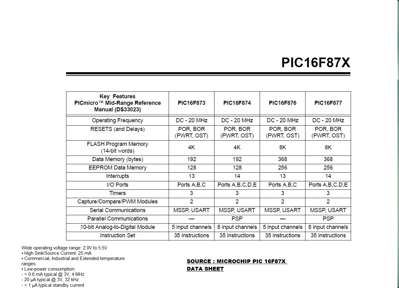
The programming of the system is done using a PIC micro controller 16F877. This powerful (200 nanosecond instruction execution) yet easy-to-program (only 35 single word instructions) CMOS FLASH-based 8-bit micro controller packs Microchip's powerful PIC® architecture into a 40-pin package and is upwards compatible with the PIC16C5X, PIC12CXXX and PIC16C7X devices. It is has five ports. I.e. port A, port B, port C, port D, port E. The PIC 16F877 has flash memory of 8K and Data memory of 368 bytes Data EEPROM of 256 bytes.The micro-controller used for our project isMicrochip’s PIC16F877A.
3.1)PIC 16F877A- FEATURES
High Performance RISC CPU:
• High performance RISC CPU
• Only 35 single word instructions to learn
• All single cycle instructions except for program branches which are two-cycle
• Operating speed: DC - 20 MHz clock input
DC - 200 ns instruction cycle
• Up to 8K x 14 words of FLASH Program Memory,
Up to 368 x 8 bytes of Data Memory (RAM)
• Interrupt capability (up to 12 sources)
• Eight level deep hardware stack
• Direct, Indirect and Relative Addressing modes
• Processor read access to program memory.
Special Microcontroller Features:
• Power-on Reset (POR)
• Power-up Timer (PWRT) and
Oscillator Start-up Timer (OST)
• Watchdog Timer (WDT) with its own on-chip RC
oscillator for reliable operation
• Programmable code protection
• Power saving SLEEP mode
Selectable oscillator options
Peripheral Features:
• Timer0: 8-bit timer/counter with 8-bit prescaler
• Timer1: 16-bit timer/counter with prescaler,
can be incremented during SLEEP via external
crystal/clock
• Timer2: 8-bit timer/counter with 8-bit period
register, prescaler and postscaler
• Two Capture, Compare, PWM modules
- Capture is 16-bit, max. resolution is 12.5 ns
- Compare is 16-bit, max. resolution is 200 ns
- PWM max. resolution is 10-bit
• 8-bit, up to 8-channel Analog-to-Digital converter
• Synchronous Serial Port (SSP) with SPI (Master
mode) and I2C (Slave)
• Universal Synchronous Asynchronous Receiver
Transmitter (USART/SCI)
• Parallel Slave Port (PSP), 8-bits wide with
external RD, WR and CS controls (40/44-pin only)
• Brown-out detection circuitry for
Brown-out Reset (BOR)
· Speed
· High Performance RISC CPU
· Instruction Set Simplicity
· Integration Of Operation Features
· Programmable Timer Options
· Interrupt Control
· EPROM /OTP/ROM options
· Inbuilt Modules
· Low Power Consumption
· Wide Operation Voltage Range :2.5to 6.0 Volt
· Programmable Code Protection Mode
· Power Saving Sleep Mode
3.2)BlockDiagramof PICMicroController
Figure2: BLOCKDIAGRAMOF PICMICROCONTROLLER
3.3)PINOUT DIAGRAM OF PIC 16F877
Figure3:PINOUT DIAGRAM OF PIC 16F877
| PIN NAME | DIP PIN # | PLCCPIN # | I/O/O TYPE | BUFFER TYPE | DESCRIP- TION | QFP |
| Osc/clkin Osc/clkout | 13 14 | 14 15 | 1 0 | St/cmos - | Osc.crystal i/p. osc.crystal o/p | 30 31 |
| MCLR/Vpp | 1 | 2 | i/p | St | Master clear i/p or program o/p. | 18 |
| RA0/AN0 RA1/AN1 RA2/AN2/VREF- RA3/AN3/VREF+ RA4/TOCK1 RA5/SS/AN4 | 2 3 4 5 6 7 | 3 4 5 6 7 8 | I/O I/O I/O I/O I/O I/O | TTL TTL TTL TTL SL TTL | Port A is bi directional i/p . | 19 20 21 22 23 24 |
| RB0/INT RB1 RB2 RB3/PGM RB4 RB5 RB6/PGC RB7/PGD | 33 34 35 36 37 38 39 40 | 36 37 38 39 41 42 43 44 | I/O I/O I/O I/O I/O I/O I/O I/O | TTL/ST1 TTL TTL TTL TTL TTL TTL/ST2 TTL/ST2 | Port B is a bi directional i/o port. Port b can be s/w pgmed for pull up on | 8 9 10 11 14 15 16 17 |
Input/output ports
PIC16F877 has 5 basic input/output ports. They are usually denoted by PORT A (R A), PORT B (RB), PORT C (RC), PORT D (RD), and PORT E (RE). These ports are used for input/ output interfacing. In this controller, “PORT A” is only 6 bits wide (RA-0 to RA-7), ”PORT B” , “PORT C”,”PORT D” are only 8 bits wide (RB-0 to RB-7,RC-0 to RC-7,RD-0 to RD-7), ”PORT E” has only 3 bit wide (RE-0 to RE-7).
PORT-A
|
RA-0 to RA-5
|
6 bit wide
|
PORT-B
|
RB-0 to RB-7
|
8 bit wide
|
PORT-C
|
RC-0 to RC-7
|
8 bit wide
|
PORT-D
|
RD-0 to RD-7
|
8 bit wide
|
PORT-E
|
RE-0 to RE-2
|
3 bit wid
|
Tbl2 :Ports in PIC 16F877A
All these ports are bi-directional. The direction of the port is controlled by using TRIS(X) registers (TRIS A used to set the direction of PORT-A, TRIS B used to set the direction for PORT-B, etc.). Setting a TRIS(X) bit ‘1’ will set the corresponding PORT(X) bit as input. Clearing a TRIS(X) bit ‘0’ will set the corresponding PORT(X) bit as output.
(If we want to set PORT A as an input, just set TRIS(A) bit to logical ‘1’ and want to set PORT B as an output, just set the PORT B bits to logical ‘0’.)
Other Pins:
o Analog input port (AN0 TO AN7) : these ports are used for interfacing analog inputs.
o TX and RX: These are the USART transmission and reception ports.
o SCK: these pins are used for giving synchronous serial clock input.
o SCL: these pins act as an output for both SPI and I2C modes.
o DT: these are synchronous data terminals.
o CK: synchronous clock input.
o SD0: SPI data output (SPI Mode).
o SD1: SPI Data input (SPI mode).
o SDA: data input/output in I2C Mode.
o CCP1 and CCP2: these are capture/compare/PWM modules.
o OSC1: oscillator input/external clock.
o OSC2: oscillator output/clock out.
o MCLR: master clear pin (Active low reset).
o Vpp: programming voltage input.
o THV: High voltage test mode controlling.
o Vref (+/-): reference voltage.
o SS: Slave select for the synchronous serial port.
o T0CK1: clock input to TIMER 0.
o T1OSO: Timer 1 oscillator output.
o T1OS1: Timer 1 oscillator input.
o T1CK1: clock input to Timer 1.
o PGD: Serial programming data.
o PGC: serial programming clock.
o PGM: Low Voltage Programming input.
o INT: external interrupt.
o RD: Read control for parallel slave port.
o CS: Select control for parallel slave.
o PSP0 to PSP7: Parallel slave port.
o VDD: positive supply for logic and input pins.
VSS: Ground reference for logic and input/output pins.
Tbl 4:specifications of the PIC 16F87X Series
The PIC 16F87x devices have a 13-bit program counter, Capable of addressing an 8K x 14 program memory space. The PIC 16F877 has 8Kx 14 words of FLASH program memory. The RESET Vector is at 0000h and the interrupt vector is at 0004h.
Data memory is partition in to multiple banks which contain the general purpose registers and special function registers. Bits RP1(status <6>) and RP0(status<5>) are the banks bits.
RP1:RP0
|
BANK
|
00
|
0
|
01
|
1
|
10
|
2
|
11
|
3
|
Tbl3: Register bank select
Each bank extends up to 7Fh (128bits). The lower location of each banks are Reserved for the special function registers. About the special function registers are general purpose registers, implemented as the static RAM. All implemented banks contain special function registers .Some frequently used special function register from 1 bank may be mirrored in another bank for code reduction and quicker access.
The analog to digital converter module has 8 inputs for the 40 pin PIC .The A/D module has 4 register :
· A/D results high register.
· A/D results low register
· A/D control register 0.
· A/D control register 1.
The A/D conversion of the analog input signals in a corresponding 10-bit digital number.
ADCON0 REGISTER.
R/W-0 R/W-0 R/W-0 R/W-0 R/W-0 R/W-0 U-0 R/W-0
ADCS 1 |
ADCON1 REGISTER
U-0 U-0 R/W-0 U-0 R/W-0 R/W-0 R/W-0 R/W-0
ADF
M
|
-
|
-
|
-
| PCF G3 | PCF G2 | PCF G1 | PCF G0 |
This mode is usually used to communicate in 8-bit ASCII code. It has two pins for transmittion and reception.Transmittion begins whenever data is written to SBUF. USART is an acronym for universal synchronous asynchronous receiver and transmitter.
Control Register Of Transmittion (Txsta)
| CS RC |
TX 9
|
TxEN
|
SYNC
|
-
|
BRGH
|
TRMT
|
Tx9D
|
Control Register Of Reception (Rxsta)
SPEN
|
Rx9
|
SREN
|
CREN
|
ADDEN
|
FERR
|
OERR
|
Rx9D
|
CHAPTER: 4
LCD DISPLAY
A liquid-crystal display (LCD) is a flat panel display, electronic visual display, or video display that uses the light modulating properties of liquid crystals. Liquid crystals do not emit light directly. LCDs are available to display arbitrary images (as in a general-purpose computer display) or fixed images which can be displayed or hidden, such as preset words, digits, and 7-segment displays as in a digital clock. They use the same basic technology, except that arbitrary images are made up of a large number of small pixels, while other displays have larger elements.
A 16x2 LCD means it can display 16 characters per line and there are 2 such lines. In this LCD each character is displayed in 5x7 pixel matrix. This LCD has two registers, namely, Command and Data.The command register stores the command instructions given to the LCD. A command is an instruction given to LCD to do a predefined task like initializing it, clearing its screen, setting the cursor position, controlling display etc. The data register stores the data to be displayed on the LCD. The data is the ASCII value of the character to be displayed on the LCD.
4.1)PINDESCRIPTION
The most commonly used LCDs found in the market today are 1Line,2Line or4 Line LCDs which have only1 controller and support at most of 80 characters, where as LCD s supporting more than 80 characters make use of 2HD44780 controllers.
Most LCD swith 1 controller has 14 Pins and LCDs with 2 controller has16 Pins (two pinsare extrainbothforback-lightLEDconnections).Pindescriptionis showninthe tablebelow.
Pin No:
|
Function
|
Name
|
1
|
Ground (0V)
|
Ground
|
2
|
Supply voltage; 5V (4.7V – 5.3V)
|
Vcc
|
3
|
Contrast adjustment; through a variable resistor
|
VEE
|
4
|
Selects command register when low; and data register when high
|
Register Select
|
5
|
Low to write to the register; High to read from the register
|
Read/write
|
6
|
Sends data to data pins when a high to low pulse is given
|
Enable
|
7
|
8-bit data pins
|
DB0
|
8
|
DB1
| |
9
|
DB2
| |
10
|
DB3
| |
11
|
DB4
| |
12
|
DB5
| |
13
|
DB6
| |
14
|
DB7
| |
15
|
Backlight VCC (5V)
|
Led+
|
16
|
Backlight Ground (0V)
|
Led-
|
Tbl 4: Pin description table of LCD module
CHAPTER: 5
ELECTRO MECHANICAL RELAYS
A relay is a switch worked by an electromagnet. It is useful if we want a small current in one circuit to control another circuit containing a device such as a lamp or electric motor which requires a large current, or if we wish several different switch contacts to be operated simultaneously.
When the controlling current flows through the coil, the soft iron core is magnetized and attracts the L-shaped soft iron armature. This rocks on its pivot and opens, closes or changes over, the electrical contacts in the circuit being controlled it closes the contacts.
The current needed to operate a relay is called the pull-in current and the dropout current in the coil when the relay just stops working. If the coil resistance R of a relay is 185 W and its operating voltage V is 12V, the pull-in current I is given by:
I = V/R = 12/185 = 65 mA
Relays are electromagnetic switches, which provides contact between two mechanical elements. Relays have a coil which works on 12V dc power supply and provides DPDT action as an output. In general relays provide potential free contacts which can be used for universal function like DC, AC voltage switching and to control bigger electrical switch gears.
The electromechanical relays are based on the comparison between operating torque/force and restraining torque/force. The VA burden of such relays are high.
The characteristics of these relays have some limitations. Each relay can perform only one protective function. Such relays are used for simple and less costly protection purposes. For important and costly equipment installation static relays are
preferred.
Figure: 5: Relay schematic diagram
Protective relaying is necessary for almost every electrical plant and no part of the power system is left unprotected.
The choice of protection depends upon several aspects such as
· type and rating of the protected equipment.
· its importance.
· location and cost.
· probable abnormal conditions between generators and final load points.
There are several electrical equipments and machines of various ratings. Each needs certain adequate protection .The protective relaying senses the abnormal conditions in a part of the power system and isolates that part from the healthy part of system.The relays used in this project are compact, self-contained devices which respond to abnormal conditions (relays can distinguish normal and abnormal conditions).The Relay driver Circuit Works as follows. A Relay is connected as shown in the figure 5(a).
The output of the controller decides Relay operation. The Relay works only if the Positive and the Ground is connected to the appropriate terminals of the relay coil. We control the relay by controlling the ground signal given to the relay using a transistor. The operation is as follows.
When the output of the controller is High, then the transistor conducts, allowing the low potential to reach one end of the relay, which results in switching of the relay form NC to NO.
When the output is Low, the transistor will not conduct. So ground is not applied to the relay Coil. So the relay remain in NC position.
Using this Normally open (NO) and Normally Closed (NC) contacts we can switch any supply AC or DC. The supply to the operated device should be given to the Common of the relay and the output from the NO is given to the Device. So that
when the relay is switched on the device gets supply and works.
CHAPTER: 6
SOLAR PANEL
6.1 )PHOTO VOLTAIC CELLS (PV CELLS)
There are two basic types of solid silicon, amorphous (having no long range order) and crystalline (where the atoms are arranged in an ordered three dimensional array). There are various other terms for the crystalline structure of silicon; poly-crystalline, micro-crystalline, nano-crystalline etc, and these refer to the size of the crystal "grains" which make up the solid. Solar cells can be, and are made from each of these types of silicon, the most common being poly-crystalline.
Silicon is a semiconductor. This means that in solid silicon, there are certain bands of energies which the electrons are allowed to have, and other energies between these bands which are forbidden. These forbidden energies are called the "band gap". The allowed and orbidden bands of energy are explained by the theory of quantum mechanics.
At room temperature, pure silicon is a poor electrical conductor. In quantum mechanics, this is explained by the fact that the Fermi level lies in the forbidden band- gap. To make silicon a better conductor, it is "doped" with very small amounts of atoms from either group 13 (III) or group 15 (V) of the periodic table. These "dopant" atoms take the place of the silicon atoms in the crystal lattice, and bond with their neighboring Si atoms in almost the same way as other Si atoms do. However, because group 13 atoms have only 3 valence electrons, and group 15 atoms have 5 valence electrons, there is either one too few, or one too many electrons to satisfy the four covalent bonds around each atom. Since these extra electrons, or lack of electrons (known as "holes") are not involved in the covalent bonds of the crystal lattice, they are free to move around within the solid. Silicon which is doped with group 13 atoms (aluminum, gallium) is known as p-type silicon because the majority charge carriers (holes) carry a positive charge, whilst silicon doped with group 15 atoms (phosphorus, arsenic) is known as n-type silicon because the majority charge carriers (electrons) are negative. It should be noted that both n-type and p-type silicon are electrically neutral,
i.e. they have the same numbers of positive and negative charges, it is just that in n-type silicon, some of the negative charges are free to move around, while the converse is true for p-type silicon.
A solar cell is a large-area semiconductor p-n junction. To understand the workings of a p-n junction it is convenient to imagine what happens when a piece of n-type silicon is brought into contact with a piece of p-type silicon. In practice, however, the p-n junctions of solar cells are not made in this way, but rather, usually, by diffusing an n- type dopant into one side of a p-type wafer.
If we imagine what happens when a piece of p-type silicon is placed in intimate contact with a piece of n-type silicon, then what occurs is a diffusion of electrons from the region of high electron concentration - the n-type side of the junction, into the region of low electron concentration - p-type side of the junction. When the electrons diffuse across the p-n junction, they recombine with holes on the p-type side. This diffusion of carriers does not happen indefinitely however, because of the electric field which is created by the imbalance of charge immediately either side of the junction which this diffusion creates. Electrons from donor atoms on the n-type side of the junction are crossing into the p-type side, leaving behind the (extra) positively charged nuclei of the group 15 donor atoms, leaving an excess of positive charge on the n-type side of the junction. At the same time, these electrons are filling in holes on the p-type side of the junction, becoming involved in covalent bonds around the group 13 acceptor atoms, making an excess of negative charge on the p- type side of the junction. This imbalance of charge across the p-n junction sets up an electric field which opposes further diffusion of charge carriers across the junction.
This region where electrons have diffused across the junction is called the depletion region because it no longer contains any mobile charge carriers. It is also known as the "space charge region". The electric field which is set up across the p-n junction creates a diode, allowing current to flow in only one direction across the junction. Electrons may pass from the n-type side into the p-type side, and holes may pass from the p-type side to the n-type side. But since the sign of the charge on electrons and holes is opposite, conventional current may only flow in one direction.
Because solar cells are semiconductor devices, they share many of the same processing and manufacturing techniques as other semiconductor devices such as computer and memory chips. However, the stringent requirements for cleanliness and quality control of semiconductor fabrication are a little more relaxed for solar cells. Most large-scale commercial solar cell factories today make screen printed poly- crystalline silicon solar cells. Single crystalline wafers which are used in the semiconductor industry can be made in to excellent high efficiency solar cells, but they are generally considered to be too expensive for large-scale mass production. Poly-crystalline silicon wafers are made by wire-sawing block-cast silicon ingots into very thin (250 to 350 micrometer) slices or wafers
The wafers are usually lightly p-type doped. To make a solar cell from the wafer, an n-type diffusion is performed on the front side of the wafer, forming a p-n junction a few hundred nanometres below the surface. Antireflection coatings, which increase the amount of light coupled into the solar cell, are typically applied next. Over the past decade, silicon nitride has gradually replaced titanium dioxide as the antireflection coating of choice because of its excellent surface passivation qualities (i.e., it prevents carrier recombination at the surface of the solar cell). It is typically applied in a layer several hundred nanometers thick using plasma-enhanced chemical vapor deposition (PECVD). The wafer is then metallised, whereby a full area metal contact is made on the back surface, and a grid-like metal contact made up of fine "fingers" and larger "busbars" is screen-printed onto the front surface using a silver paste. The rear contact is also formed by screen-printing a metal paste, typically aluminum. Usually this contact covers the entire rear side of the cell, though in some cell designs it is printed in a grid pattern. The metal electrodes will then require some kind of heat treatment or "sintering" to make Ohmic contact with the silicon. After the metal contacts are made, the solar cells are interconnected in series (and/or parallel) by flat wires or metal ribbons, and assembled into modules or "solar panels".
Solar panels have a sheet of tempered glass on the front, and a polymer encapsulation on the back. Some solar cells have textured front surfaces that, like antireflection coatings, serve to increase the amount of light coupled into the cell. Such surfaces can usually only be formed on single-crystal silicon, though in recent years methods of
These are also known as solar cells and their assembly is termed as solar panel, let us see the individual discrete component of solar cell which is shown in below Fig
Figure 7: STRUTURE OF SOLAR CELL
PV cells were invented in 1953 by Charles Fariett. A PV cell is used for converting photon into electron and with sun light incident, electrical energy is generated. The solar-based battery may be used to directly feed electricity to electronic equipment or for domestic heating. Solar batteries can also be used for satellites, communication equipment and domestic appliances.
A selenium-or silicon-based solar cell exhibits open-circuit voltage of only 0.5V and short-circuit cell current of the order of 1milliampere for 6.4cm² area of the cell at6458 meter candles. Therefore a large number of such silicon or selenium solar cells need to be connected in series and parallel to provide any significant power. A telemetry system required to operate 24 hours a day requires a solar panel providing 5 watts at 12 volts used for recharging corresponding storage batteries during daylight hours.
CHAPTER: 7
RECHARGEABLE BATTERY
A rechargeable battery, storage battery, or accumulator is a type of electrical battery. It comprises one or more electrochemical cells, and is a type of energy accumulator. It is known as a secondary cell because its electrochemical reactions are electrically reversible. Rechargeable batteries come in many different shapes and sizes, ranging from button cells to megawatt systems connected to stabilize an electrical distribution network. Several different combinations of chemicals are commonly used, including: lead–acid, nickel cadmium (NiCd),nickel metal hydride (NiMH), lithium ion (Li-ion), and lithium ion polymer (Li-ion polymer).
Rechargeable batteries have lower total cost of use and environmental impact than disposable batteries. Some rechargeable battery types are available in the same sizes as disposable types. Rechargeable batteries have higher initial cost but can be recharged very cheaply and used many times
7.1)Charging and discharging
During charging, the positive active material is oxidized, producing electrons, and the negative material is reduced, consuming electrons. These electrons constitute the current flow in the external circuit. The electrolyte may serve as a simple buffer for internal ion flow between the electrodes, as in lithium-ion and nickel-cadmium cells, or it may be an active participant in the electrochemical reaction, as in lead–acid cells.
Figure 9:Diagram of the charging of a secondary cell battery.
The energy used to charge rechargeable batteries usually comes from a battery charger using AC mains electricity, although some are equipped to use a vehicle's 12-volt DC power outlet. Regardless, to store energy in a secondary cell, it has to be connected to a DC voltage source. The negative terminal of the cell has to be connected to the negative terminal of the voltage source and the positive terminal of the voltage source with the positive terminal of the battery. Further, the voltage output of the source must be higher than that of the battery, but not much higher: the greater the difference between the power source and the battery's voltage capacity, the faster the charging process, but also the greater the risk of overcharging and damaging the battery.
Chargers take from a few minutes to several hours to charge a battery. Slow "dumb" chargers without voltage- or temperature-sensing capabilities will charge at a low rate, typically taking 14 hours or more to reach a full charge. Rapid chargers can typically charge cells in two to five hours, depending on the model, with the fastest taking as little as fifteen minutes. Fast chargers must have multiple ways of detecting when a cell reaches full charge (change in terminal voltage, temperature, etc.) to stop charging before harmful overcharging or overheating occurs. The fastest chargers often incorporate cooling fans to keep the cells from overheating.
Battery charging and discharging rates are often discussed by referencing a "C" rate of current. The C rate is that which would theoretically fully charge or discharge the battery in one hour. For example, trickle charging might be performed at C/20 (or a "20 hour" rate), while typical charging and discharging may occur at C/2 (two hours for full capacity). The available capacity of electrochemical cells varies depending on the discharge rate.
CHAPTER : 8
CIRCUIT DIAGRAM
Figure:CIRCUIT DIAGRAM
8.1)CIRCUIT DIAGRAM EXPLANATION
Here we are using PIC16F877Aas the major component. Which will control all actions and provide basic protection based on the program.
The current produced by the solar panel is flowing to the battery through a relay switch RL1. When the battery is fully charged RL1 will be energised and disconnects the solar panel from battery .The relay switch RL2 is used to protect the battery from over load. When an overload is occurred, the relay switch RL2 is energised and it disconnects load from battery.
The relay will be de-energised when the overload reset switch is pressed. The voltage at the battery is continuously displayed on the LCD using the built-in ADC module in the PIC 16F877A. The voltage is divided by 3 by using 3 equal value resistors and 1/3 voltage is send to ADC input. The analogue voltage is converted into digital and it is displayed on LCD after multiplying with 3. The reference voltage for the ADC conversion is taken from the VDD supply.
The rated current of the power supply is chosen as 3A. At full load, the load voltage will be 9.6V (full load resistance = V/I = 12V/3A = 4Ohm. Therefore Load voltage = 12 x 4/5 = 9.6V using voltage divider rule) it is divided by 3 using resistive network and given to ADC channel 2(AN2). The voltage is continuously measured by the pic. If over load occurs, the voltage at load reduces. It is detected by the pic and energises relay switch 2 and disconnects load from over current.
CHAPTER: 9
PROGRAM CODING
sbit LCD_RS at RB0_bit;
sbit LCD_EN at RB1_bit;
sbit LCD_D4 at RB2_bit;
sbit LCD_D5 at RB3_bit;
sbit LCD_D6 at RB4_bit;
sbit LCD_D7 at RB5_bit;
sbit LCD_RS_Direction at TRISB0_bit;
sbit LCD_EN_Direction at TRISB1_bit;
sbit LCD_D4_Direction at TRISB2_bit;
sbit LCD_D5_Direction at TRISB3_bit;
sbit LCD_D6_Direction at TRISB4_bit;
sbit LCD_D7_Direction at TRISB5_bit;
float b;
float a;
char txt[10];
void main()
{
trisa=0xff;
trisc=0xff;
trisd=0x00;
Lcd_Init();
Lcd_Cmd(_LCD_CURSOR_OFF);
delay_ms(200);
ADC_Init();
delay_ms(200);
while(1)
{
a=.00488*ADC_Read(0)*3;
FloatToStr(a, txt);
strcat(txt,"V");
Lcd_Out(1,2,"SOLAR CHARGER");
Lcd_Out(2,4,txt);
//Lcd_Out(2,6,"v");
delay_ms(300);
if(a>12)
portd.f7=0;
else
portd.f7=1;
b=.0048*ADC_Read(1);
/*Lcd_Out(1,1,"load");
FloatToStr(b, txt);
Lcd_Out(2,1,txt);
delay_ms(1000);*/
if(b<3)
{
Lcd_Cmd(_LCD_CLEAR);
Lcd_Out(1,4,"OVER LOAD");
portd.f6=1;
while(portc.f0==1);
portd.f6=0;
}
else
portd.f6=0;}}
CHAPTER : 10
PCB FABRICATION AND SOLDERING
Printed Circuit Board (PCB) is piece of art. The performance of an electronic circuit depends on the design and layout of the PCB. A PCB mechanically supports and connects components by conductive pathways, etched from copper sheets laminated on to insulated substrate. PCB are used to rotate electrical currents and signals through copper tracts which are firmly bonded to an insulating base.
PCB fabrication involves following steps:
1. Drawing the layout of the PCB in the paper. The track layout of the electronic circuit should be made in such manner that the paths are in easy routes. It is then transferred to a Mylar sheet. The sheet is then touched with black ink.
2. The solder side of the Mylar sheet is placed on the shiny side of the five-star sheet and is placed in a frame. Then it is exposed to sunlight with Mylar sheet facing the sunlight.
3. The exposed five-star sheet is put in hydrogen peroxide solution. Then it is put in hot ater and shook till unexposed region becomes transparent.
4. This is put in cold water and then the rough side is stuck onto the silk screen. This is then pressed and dried well.
5. The plastic sheet of the five-star sheet is removed leaving the pattern on the screen.
6. A copper clad sheet is cut to the size and cleaned. This is placed under screen.
7. As it resistant ink if spread on the screen so that a pattern of tracks and a pad is obtained on a copper clad sheet. It is then dried.
8. The dried sheet is then etched using ferric chloride solution
9. (32Baume) till all the unwanted copper is etched away. Swish the board to keep the each fluid moving. Lift the PCB and check whether all the unwanted copper is removed. Etching is done by immersing the marked copper clad in ferric chloride solution. After that the etched sheet is dried.The unwanted resist ink is removed using sodium hydroxide solution Holes are then dried.
PCB PARAMETERS
Copper thickness- 72mil (1mm=39.37mils)
Track width- 60 mil
Clearance - 60 mil
Pad width- 86mil
Pad height - 86 mil
Pad shape- oval
Pad hole size- 25mil
On board- Through
Hole size- .9mm(36mil)
Base - paper phenolic, hylam
PCB Quality- FRC
SOLDERING
Soldering is the process of joining metals by using lower melting point to weld or alloy with joining surface.
SOLDER:
Solder is the joining material that melts below 427 degree connections between components.The popularly used solders are alloys of tin(Sn) and lead(Pb) that melts below the melting point if tin.
Types:
1. Rosin core: - 60/40 Sn/Pb solders are the most common types used for electronics assembly. These solders are available in various diameters and are most appropriate for small electronics work(0.02”-0.05|| dia is recommended)
2. Lead free :- Lead free solders are used as more environmental-friendly substitutes for leaded solder, but they are typically not as easy to use mainly because of their higher melting point and poorer wetting properties.
3. Silver:- Silver solders are typically used for low resistance connections but they have a higher melting point and are expensive than Sn/Pb solders.
4. Acid-core:- acid-core solders should not be used for electronics.They are intended for plumbing of non-electronics assembly work. The acid-core flux will cause corrosion of circuitry and can damage components.
5.Other special solders:- various melting point eutectics: these
6.special solders are typically used for non-electronic assembly of difficult to construct mechanical items that must be assembled in a particular sequence .
FLUX
In order to make the surface accept the solder readily ,the components terminals should be free oxides and other obstructing films .the lead should be cleaned chemically or by abrasion using blades or knives. Small amount of lead coating can be done on the portion of the leads using soldering iron .this process is called thinning. Zinc chloride or ammonium chloride separately or in combination is mostly used as fluxes. These are available in petroleum jelly as paste flux. The desirable properties of flux are:-
It should provide a liquid cover over the materials and exclude air gap up to the soldering temperature. It should dissolve any oxide on the metal surface. It should be easily replaced from the metal by the molten soldering operation.Residue should be removable after completing soldering operation.The most common flux used in hand soldering of electronic components is rosin, a combination of mild organic acids extracted from pine tree.
SOLDERING IRON
It is a tool used to melt the solder and apply it at the joints in the circuit. it operates in 230V supply. The iron at the tip gets heated while few minutes. 50W and 25W soldering irons are commonly used for soldering of electronics circuit.
SOLDERING STEPS
1. Make the layout of the component in the circuit. Plug in the chord of the soldering irons the main to get heated.
2. Straighten and clean the component leads using a blade or knife.
3. Mount the components on the PCB by bending the leads of the components. Use nose pliers.
4. Apply flux on the joints and solder the joints. Solder must be in minimum time to avoid dry soldering and heating up of the components.
5.Wash the residue using water and brush.
6.Solder joints should be inspected when completed to determine if they have been properly made.
CHARACTERISTICS OF A GOOD SOLDER JOINTS:
A. Shiny surface
B. Good, smooth fillet
CHARACTERISTICS OF A POOR SOLDER JOINTS:
1. Dull or crystallized surface: This is an indicator of a cold solder joint. Cold solder joint result from moving the component after soldering has been removed, but before the solder has hardened. Cold solder joints may work at first, but will eventually fail.
2. Air Pocket: Air pocket (voids) result from incomplete wetting of surface, allowing air to be in contact with the connecting metals. This will cause oxidation of the joints & eventual failure. Blow holes can occur due to vaporization of moisture on the surface of the board & existing through the molten solder. Boards should be clean & dry, prior to soldering. Ethanol (100%) can be used as a moisture chaser if boards are wet prior to soldering.
3. Dimples: Dimples in the surface do not always indicate a serious problem, but they should be avoided since they are precursors to voids.
4. Floaters: Black spots-Floating in the soldering fillet should be avoided, because they indicate contamination & potential for failure as in the case of voids. These black spots usually results from overheated (burnt) Rosin or other contaminants such as burnt wire insulation. Maintaining a clean tip will help to avoid these problems.
5.Balls:A solder balls instead of a fillet can occur if the trace was heated but the leads were not(vice versa).This prevents proper wetting of both surfaces & result in solder being attached to only one surface(component of trace).
6. Excess solder: Excess solder usage can cover up other potential problems & should be avoided. It can lead to solder bridges. In addition, spherical solder joints can result from the application of too much solder
PCB LAYOUT
Figure: PCB LAYOUT
CHAPTER : 11
SOFTWARES USED
Ø PROTHEUS
Proteus is a software for microprocessor simulation, schematic capture, and printed circuit board (PCB) design. It is developed by Labcenter Electronics.The XGameStation Micro Edition was designed using Labcenter's Proteus schematic entry and PCB layout tools
Proteus PCB design combines the ISIS schematic capture and ARES PCB layout programs to provide a powerful, integrated and easy to use suite of tools for professional PCB Design.All Proteus PCB design products include an integrated shape based autorouter and a basic SPICE simulation capability as standard. More advanced routing modes are included in Proteus PCB Design Level 2 and higher whilst simulation capabilities can be enhanced by purchasing the Advanced Simulation option and/or micro-controller simulation capabilities.
System components
· ISIS Schematic Capture - a tool for entering designs.
· PROSPICE Mixed mode SPICE simulation - industry standard SPICE3F5 simulator combined with a digital simulator.
· ARES PCB Layout - PCB design system with automatic component placer, rip-up and retry auto-router and interactive design rule checking.
· VSM - Virtual System Modelling lets cosimulate embedded software for popular micro-controllers alongside hardware design.
· System Benefits Integrated package with common user interface and fully context sensitive help.
Ø MIKRO C
MikroC is a full-featured ANSI C compiler that is available for six different microcontroller architectures (in this case, for PIC 12/16/18). It features an intuitive IDE, a powerful compiler with advanced SSA optimizations, lots of hardware and software libraries, and additional tools that will help you in your work. The compiler comes with a comprehensive Help file (700 pages) and lots of ready-to-use examples designed to get you started in no time.
Each compiler license includes free upgrades and tech support for the lifetime of the product. The software features a Live Update service so you can get new features and improvements instantly.
The mikroC PRO for PIC compiler supports 504 PIC microcontrollers. Newly released PIC microcontrollers will be supported by new versions of the compiler software that is updated regularly.
The compiler is designed to be smart and efficient, so you can rely on it to do the hard work. It features four levels of optimizations that can reduce your code size up to 20 percent. Standard header files are included that make it easy to port your code from other C compilers.
MikroC PRO for PIC C Compiler Features
Single-click Debugging
mikroC PRO for PIC has native support for the mikroICD In-Circuit Debugger feature of the fast USB 2.0 mikroProg-PIC programmer (in both on-board and standalone versions). mikroICD is a separate DLL module which supports Step-over, Step-Into, Step-Out, Run, and Run-to-Cursor debugging operations. Also, the debugger supports standard and advanced breakpoints.
Faster, better, more productive
mikroC PRO for PIC comes equipped with fully functional software tools that can boost your efficiency and do the job for you, so you can be more productive in your work: LCD Custom Character Tool, GLCD Bitmap Editor, Seven-Segment Editor, UART Terminal, UDP Terminal, HID Terminal, ASCII Chart, Active Comments Editor, Advanced Statistics and more.
No comments:
Post a Comment